What a Single Field Return Tells You About Missing Circuit Protection
Most electronics teams have seen this kind of failure: a customer returns a PCB assembly that “just died,” with no smoke, no visible burn marks, and no sign of mechanical damage. The product passed bench testing, shipped successfully, and only later failed in the field. What appears to be one isolated complaint is often a sign of a broader margin problem.
A field return is not just one bad unit. It is a sample from a production population exposed to the same electrical stress. If one board was damaged by a transient on the input rail, other units likely saw the same condition. This failed unit simply fell on the wrong side of the tolerance stack, due to factors such as higher line voltage, a lower-margin MOSFET, a load step during switching, or parasitic inductance that caused overshoot. Without a defined protection strategy, reliability is left to tolerances and chance.
The key question is where the fault energy went. In a protected design, a TVS clamps the transient, a PPTC or fuse limits current, and the MCU either rides through the event or resets cleanly. In an unprotected design, the energy still enters the system but finds the weakest node, such as a gate oxide, PCB trace, connector pin, or capacitor. The failure may look random, but it is actually deterministic.
This is why missing protection is so costly to debug. Without a protection device in the fault path, there is no controlled failure mode and no clear indicator of root cause. One RMA should therefore trigger a protection review: identify the fault source, source impedance, available energy, and stress path, then match them to the right protection parameters. A single field return is not an outlier. It is an early warning that the design may lack defined behavior under electrical stress.
Circuit Protection Threats Electronic Products Must Be Designed Against
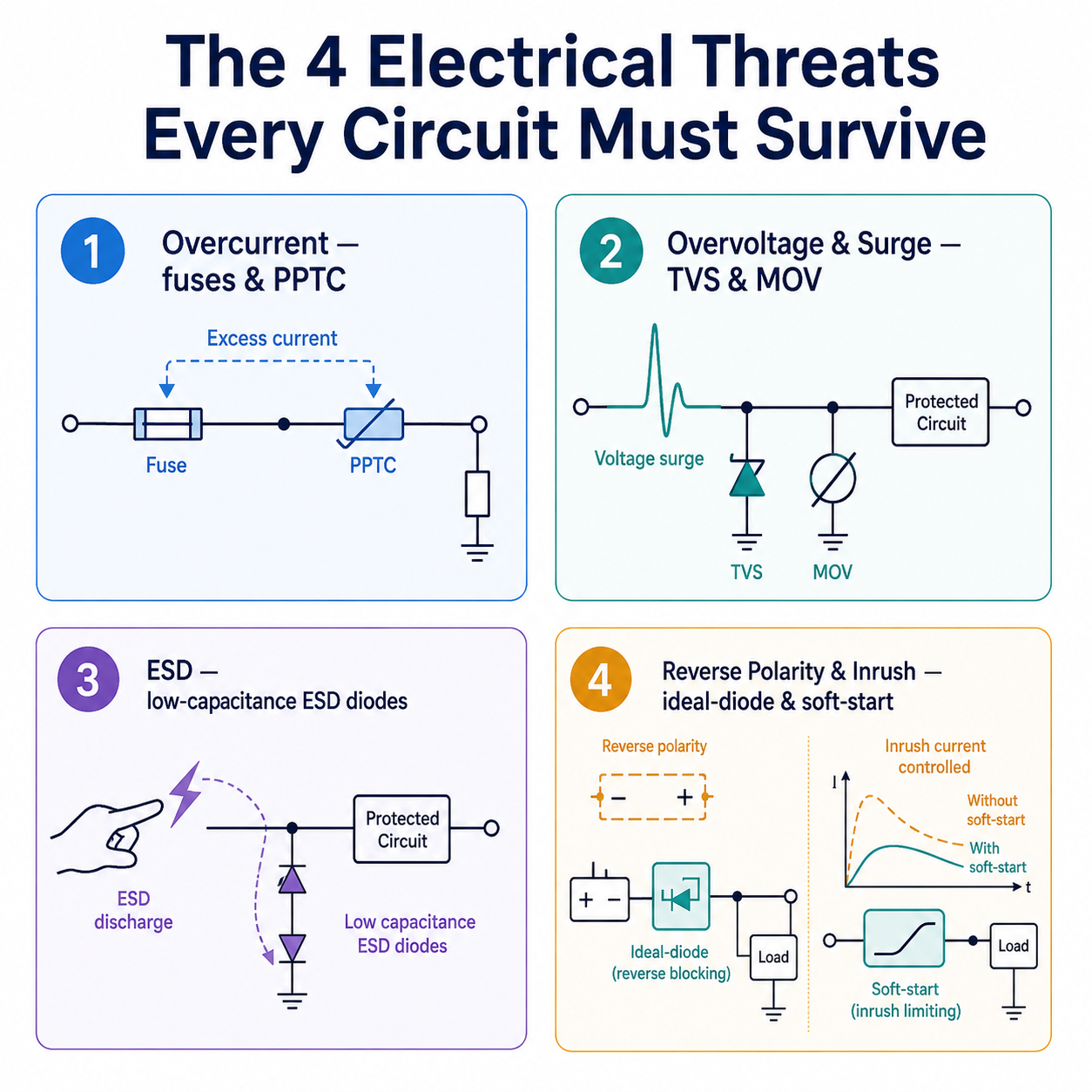
Before selecting a protection component, define the threat. “The board died” is not a fault mode; it is an outcome. In practice, most field failures that circuit protection is intended to prevent trace back to four categories of electrical stress. They differ in energy content, rise time, duration, and entry point, and those differences determine the correct protection device and placement.1. Overcurrent
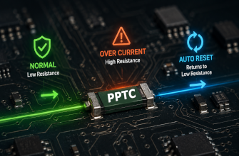
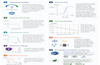
Overcurrent is excessive current through a path that was not designed to carry it. Typical causes include downstream short circuits, failed loads, stalled motors, wiring faults, connector mis-mating, or components that fail short over time. The primary hazard is thermal: copper traces heat up, solder joints can reflow, connectors can overheat, and in severe cases a trace or connector can become an ignition source.Overcurrent protection is usually implemented with fuses, resettable PPTC devices, current limiters, or electronic protection switches. For a PPTC, the key parameters include hold current (I_H), trip current (I_T), resistance over temperature, time-to-trip, maximum voltage, and maximum fault current. For a fuse, the selection normally centers on rated current, voltage rating, interrupting rating, time-current curve, and I²t let-through energy. The engineering decision is whether the fault should recover automatically after it clears, or whether the system should latch open and require service.
2. Overvoltage, Transients, and Surges
Overvoltage stress is a voltage excursion above the safe operating range of the protected circuit. It can come from inductive load switching, relay or motor commutation, nearby lightning-induced surges, supply misconnection, hot-plug events, or automotive load dump. The failure mechanism is often dielectric breakdown or junction overstress: MOSFET gate oxides, IC input structures, regulators, and capacitors are rated for specific voltages, not for arbitrary transient excursions.This is the domain of transient-voltage suppressors, MOVs, and coordinated clamp networks. A TVS diode provides fast, repeatable clamping and is typically selected by working standoff voltage (V_RWM), breakdown voltage, clamping voltage (V_CL) at a specified pulse current, peak pulse power (P_PP), and the relevant surge waveform. An MOV can absorb higher surge energy at attractive cost, but it has a softer clamping characteristic and degrades with surge exposure. The core design task is coordination: the clamp must turn on early enough and keep the protected node below the downstream absolute maximum rating for the full pulse duration, not only at the waveform peak.
3. Electrostatic Discharge (ESD)
ESD is the fastest and often the most underestimated threat. A human-body or charged-device discharge can reach kilovolt-level potentials with sub-nanosecond edge rates and can enter through USB, Ethernet, buttons, antennas, connectors, display interfaces, or enclosure seams. At those rise times, package inductance, trace inductance, return-path geometry, and placement are as important as the protection silicon itself.Dedicated ESD protection devices are selected by reverse working voltage, dynamic resistance, clamping voltage at the relevant ESD current, IEC 61000-4-2 robustness, leakage current, and line capacitance. Capacitance is especially critical for high-speed interfaces because a device that protects the port but degrades the signal integrity is not an acceptable design solution. ESD damage may not always cause an immediate hard failure; it can degrade input structures over many strikes and later appear as an intermittent or “no trouble found” field return.
4. Reverse Polarity and Inrush Current
The fourth category is connection and power-up abuse. Reverse polarity can result from a miswired supply, an incorrectly installed battery, or a field wiring error. Inrush current occurs when bulk capacitance charges during hot-plug or power application. Both can create stress conditions that steady-state design calculations never see. A reversed supply can destroy downstream circuitry in milliseconds, and uncontrolled inrush can pit connectors, collapse upstream supplies, or nuisance-trip upstream protection.Reverse-polarity protection may use a series diode, a Schottky diode where loss is acceptable, or an ideal-diode controller / MOSFET arrangement where voltage drop and efficiency matter. Inrush is commonly managed with an NTC thermistor, active current limiting, a hot-swap controller, or a soft-start circuit. These functions belong in the same protection review because they answer the same engineering question: what is the worst electrical condition that can reach each node, and what component or circuit is responsible for controlling it?
Once these four threat categories are mapped against the product environment, the protection architecture becomes much easier to define.
Consequences of Leaving Circuit Protection Out: Safety, Warranty, and Brand Risk
Removing a protection component may save a few cents on the BOM, but it usually transfers cost to places that are harder to see during design review. The real tradeoff is not “protection versus no protection.” It is a known, bounded cost at design time versus an unknown, compounding cost after shipment.Safety: The Failure Mode You Cannot Afford
The first cost is physical safety. A sustained overcurrent that is not interrupted can turn copper, connectors, and harnesses into heat sources. An unclamped surge can rupture a capacitor, overstress insulation, or damage an IC in a way that creates a secondary hazard. A product that fails safe - by clamping, current-limiting, browning out, or opening a protective element - creates an inconvenience. A product that fails into an ignition source, an exposed hazardous voltage, or an uncontrolled thermal event can trigger a recall, a regulatory finding, or loss of market access.This is why protection strategy is closely tied to standards and certification. UL, IEC, automotive, industrial, and medical requirements generally expect defined behavior under abnormal operation and single-fault conditions. Certification is not based on the assumption that faults will not occur; it is based on demonstrating that the product remains safe when they do occur. Leaving protection out can therefore turn a reliability issue into a compliance issue.
Warranty: A Cost That Scales with Volume
The second cost is financial, and it scales in the wrong direction. A TVS, PPTC, fuse, MOV, or ESD diode is a predictable per-unit cost. A field failure is a variable cost that grows with installed base and time in service: two-way freight, replacement hardware, service labor, customer support time, FA lab time, engineering escalation, buffer inventory, and corrective-action overhead. A ten-cent protection device removed from a 100,000-unit program does not simply save ten thousand dollars; it exposes the program to an unbounded return rate and the full cost of each return.There is also a diagnostic multiplier. Without a protection component in the fault path, the failure mode is uncontrolled, so every return tends to consume more engineering time. You are not only paying for more failures; you are paying more per failure because the evidence is less readable.
Brand: The Cost That Does Not Show Up as a Line Item
The third cost is reputation. A customer who receives a dead unit does not attribute the failure to marginal source impedance, weak transient immunity, or component tolerance. The customer simply concludes that the product is unreliable. Distributor confidence, design-in opportunities, online reviews, and repeat purchases are driven by perceived reliability, and perceived reliability is set by the worst field experiences, not by the median unit.
A product that consistently survives misuse and electrical abuse strengthens a supplier’s reputation for robust engineering. A pattern of unexplained field deaths does the opposite. Unlike warranty cost, brand damage cannot be cleanly refunded or reserved against; by the time it appears in sales data, it has already affected the next design-in decision.
Taken together, the logic is straightforward: safety failures can stop a product line, warranty failures scale with shipment volume, and brand damage outlives the individual units that caused it. Circuit protection devices are usually among the lowest-cost components on the board, but they can prevent the highest-consequence failure modes.
What a Basic Circuit Protection Architecture Looks Like
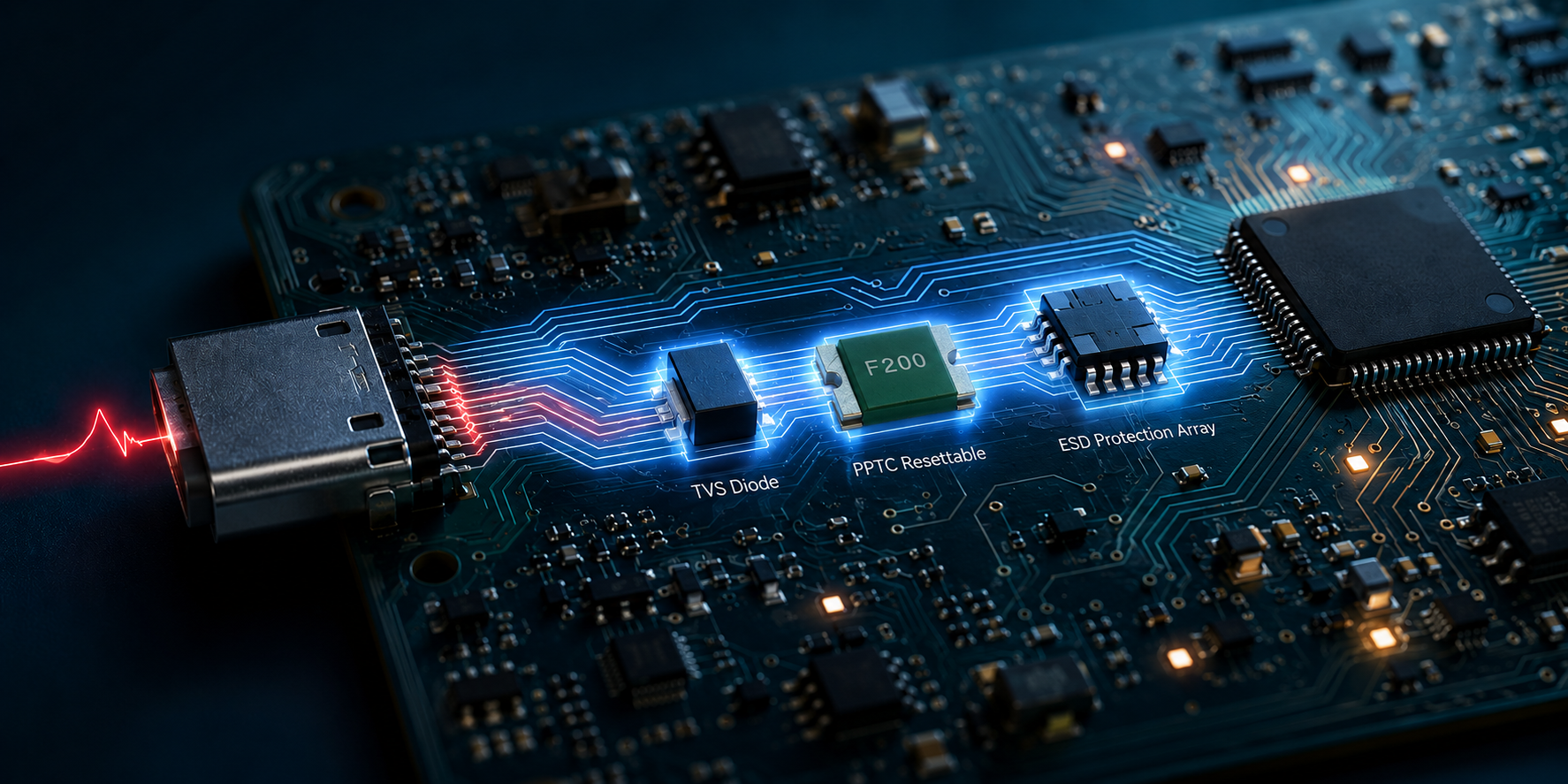
Once the threats are defined, protection should not be a random collection of parts. It should be a coordinated architecture from the connector inward. Each layer should handle the stress it is best suited to absorb before that stress reaches more fragile circuitry.At the Connector: Clamp Fast Events and Block Wrong-Way Power
The connector or external interface is the first point of entry for most faults, so it is where the fastest and most direct threats should be handled. ESD protection devices belong as close as practical to exposed pins. A TVS diode on the input rail should be placed near the power-entry point, with a low-inductance path to the appropriate return or chassis reference. Placement is not cosmetic: every millimeter of trace between the connector and the clamp adds inductance and allows voltage overshoot before the clamp becomes effective.Reverse-polarity protection also belongs near the input boundary. A reversed supply should be blocked before it energizes downstream regulators, ICs, or load switches. Depending on efficiency and voltage-drop requirements, that function may be implemented with a diode, a MOSFET ideal-diode circuit, or a dedicated controller.
On the Power Rail: Limit Fault Current and Shunt Surge Energy
Behind the input boundary sits the power-rail protection layer. A fuse, PPTC resettable fuse, eFuse, or hot-swap controller limits fault current in the main rail. In parallel, a TVS or MOV shunts surge energy and keeps the rail below the downstream absolute maximum limits. The series element and shunt element must be selected together. The clamp diverts the transient energy; the series device limits the available current and protects traces, connectors, and the clamp itself from sustained overload.If inrush is a concern, this is also where the soft-start, NTC thermistor, active inrush limiter, or hot-swap function belongs. The goal is to make the power rail behave predictably during both steady-state operation and abnormal connection events.
At the Load: Protect High-Value and Low-Margin Silicon
The final protection layer sits close to sensitive loads: the MCU, RF front end, gate driver, sensor input, high-speed interface, or low-voltage regulator. These devices often have the lowest absolute maximum ratings and the least tolerance for overshoot. Upstream protection handles bulk energy, while local protection handles residual voltage, ringing, and high-frequency energy that passes through the upstream network because of parasitic inductance and layout impedance.For data and RF lines, the local device must also preserve signal integrity. That means low capacitance, low leakage where required, appropriate bandwidth, and a layout that routes the strike current away from the protected signal path.
The Key Engineering Task: Coordination
Layered protection works only when the ratings are coordinated. Each clamp’s working standoff voltage must be above the maximum normal operating voltage so it does not conduct during normal operation. Its clamping voltage must be below the protected component’s absolute maximum rating with adequate margin under the actual pulse condition. The current-limiting element must carry the real load current, including startup and temperature effects, without nuisance tripping, yet it must open or limit current before the trace, connector, cable, or shunt device overheats.A TVS that clamps at 40 V does not protect a 30 V-rated IC input. A PPTC with an I_H below the real peak load current will trip during normal operation. An MOV that absorbs the first surge but leaves too much residual voltage for the downstream silicon is not sufficient by itself. The components are inexpensive; making their ratings nest correctly is the engineering work.
A practical baseline is three coordinated gates: clamp and block at the connector, limit and absorb on the power rail, and provide local clamping at the load. With the right sequence and ratings, the board has defined behavior for each major electrical threat instead of leaving the outcome to the weakest node.
Circuit Protection Priorities by Product Type
The same four threats apply across products, but their priority changes with the use environment, power source, interface exposure, and applicable standards. Good engineering does not protect everything equally; it spends cost and board area where the stress energy and compliance risk are highest.Consumer and Portable Devices: ESD First, Capacitance Matters
Products that users touch and plug in repeatedly - phones, wearables, USB accessories, handheld instruments, and consumer peripherals - are dominated by exposed-interface ESD. Every connector, button, antenna feed, and enclosure seam can become an ESD entry point over the product life. Low-capacitance ESD protection should be placed close to accessible pins, especially on high-speed data lines.Input overvoltage from adapters or chargers also matters, but the common selection trap is capacitance. A large general-purpose TVS may protect a port electrically while degrading USB, RF, or high-speed serial performance. For these designs, the typical priority is ESD protection first, then input overvoltage, with current limiting often integrated into the charger IC, PMIC, or port controller.
Automotive Electronics: Harsh Supply Rails and Overvoltage Immunity
Automotive designs are dominated by a harsh electrical environment. A nominal 12 V rail is not simply 12 V; it can experience load dump, jump-start conditions, alternator ripple, inductive switching noise, cold-crank sag, and reverse-battery events. The protection network must be designed against the relevant ISO and OEM transient profiles rather than against the nominal voltage alone.A robust automotive input may require a load-dump-rated TVS, an MOV or staged clamp for high-energy events, reverse-polarity protection, and careful thermal derating. Ambient temperature is not a footnote. A protection device rated at 25 °C can behave very differently at under-hood or enclosed-module temperatures. The priority is supply overvoltage immunity, reverse-battery protection, and verified derating across the operating temperature range.
Industrial Equipment: Fault Current, Long Cables, and Surge Coupling
Industrial equipment typically operates at higher power levels and connects through long cables. That increases available fault current and creates more opportunities for inductive or lightning-related surge coupling. Interrupting rating matters: a fuse that cannot safely clear the available fault current is not a valid protection device for that location.Long signal and power lines can behave like antennas for coupled surge energy, so ports often need protection sized for surge events rather than only for ESD. Communication interfaces may also require galvanic isolation, common-mode surge protection, and coordination with earth/chassis bonding. The usual priority is overcurrent protection with adequate interrupting rating, line-surge suppression, and isolation where the system standard or installation environment requires it.
Medical and Safety-Critical Systems: Defined Failure and Documented Margin
For medical, safety-critical, and mission-critical equipment, the priority is not only a particular electrical threat; it is demonstrable safe behavior under fault. The design must fail into a known safe state, and the margin must be documented well enough to survive a design review, risk analysis, or certification audit.That usually means conservative derating, redundancy where required, monitored fault paths, and protection coordination that can be traced to actual fault assumptions. The lowest-cost component is not acceptable if its ratings cannot be justified under the use case. The priority is defined fail-safe behavior, documented derating, and protection coordination before component cost optimization.
Battery-Powered IoT: Leakage and Quiescent Current
Small battery-powered products have a different constraint: the protection network cannot consume the battery life it is supposed to protect. Every clamp has leakage, every series element has resistance, and every active protection IC has quiescent current. In coin-cell and low-duty-cycle IoT devices, microamps matter.ESD and overvoltage protection still matter at exposed interfaces, but leakage current, capacitance, and series resistance become first-order parameters. The priority is low-leakage ESD/TVS protection, current limiting matched to the actual low load current, and avoidance of always-on circuits that consume unnecessary standby power.
Across all product types, the method is the same: inventory the threats, rank them by likelihood and energy for the actual environment, and allocate the protection budget where the electrical stress is real.
FAQ
Can I just add a fuse and call the design protected?
No. A fuse primarily addresses sustained overcurrent. It does not clamp an overvoltage transient, stop ESD, or correct reverse polarity, and it is generally too slow to protect silicon from a fast surge. Fuses and PPTCs limit fault current to prevent overheating. TVS diodes, MOVs, and ESD devices limit voltage to prevent dielectric breakdown and junction overstress. They address different physics and are typically used together, not as interchangeable parts.PPTC or Fuse: How Should I Choose?
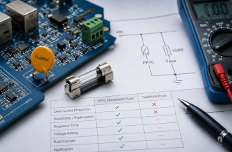
Start with the desired fault behavior. A PPTC resettable fuse increases resistance during a fault and can recover after the fault is removed and the device cools, which is useful for transient overloads such as temporary stalls, hot-plug events, or user-recoverable faults. A fuse is one-shot and is appropriate when a hard fault should remain disconnected until service. Select a PPTC by I_H, I_T, resistance, time-to-trip, voltage rating, and temperature derating. Select a fuse by rated current, voltage rating, interrupting rating, time-current characteristic, and I²t.TVS or MOV for Surge Protection?
A TVS diode provides fast and relatively precise clamping, making it well suited for protecting sensitive electronics. An MOV generally absorbs higher surge energy per cost but clamps less precisely and degrades with repeated surge exposure. High-energy designs often use both: an MOV or other front-end device handles the bulk surge energy, and a downstream TVS limits the residual voltage seen by the protected circuit. Selection should be based on the actual surge waveform, source impedance, repetition rate, and allowed residual voltage, not on a generic surge rating.What Clamping Voltage Should I Target?
Work backward from the protected component. Identify the absolute maximum rating of the vulnerable node, apply an appropriate derating margin, and keep the clamp voltage below that ceiling under the specified pulse condition. Then confirm that the working standoff voltage remains above the maximum normal operating voltage so the clamp does not conduct during normal operation. The useful window is between the highest normal rail voltage and the protected device’s safe limit.Does Layout Really Matter for ESD?
Yes. At ESD rise times, layout can determine whether the protection device is effective. Place the ESD device close to the connector pin, keep the discharge path to ground or chassis short and low inductance, avoid routing the protected signal past the clamp and then back again, and provide a return path that does not force strike current through sensitive circuitry. A good ESD diode placed poorly can fail to protect the node it is intended to protect.How Much Derating Should I Use?
Use enough derating that no component operates at its limit during normal or credible worst-case conditions. Voltage, current, power, surge energy, temperature, and repetition rate all interact. A TVS specified at 25 °C may have reduced power capability at 85 °C or 125 °C. A PPTC’s hold current changes significantly with ambient temperature. Derating must be checked at the real operating temperature and installation condition, not only at the datasheet reference condition.Where Should I Start on a New Design?
Start by defining the fault environment for each interface and rail: available fault current, surge waveform, source impedance, edge rate, maximum normal voltage, expected ambient temperature, and the absolute maximum ratings of the circuits being protected. Then choose devices from the connector inward and verify that adjacent clamps and current-limiting elements coordinate. Selecting protection parts before quantifying the threat is how a design ends up looking protected on the schematic while remaining vulnerable in the field.Can PPTC, TVS, MOV, and fuses be used together?
Yes. Multi-stage circuit protection is common when the product must survive more than one fault class. A shunt device such as a TVS or MOV limits voltage, while a series device such as a PPTC, fuse, eFuse, or hot-swap controller limits sustained current. The key is coordination. The clamp must keep the protected node below its safe limit, the series element must survive normal load and startup conditions, and the two devices must not force each other into thermal or surge overstress. Verify standoff voltage, clamping voltage, I²t, time-to-trip, interrupting rating, pulse repetition, and temperature derating as a system.How do I choose between PPTC, TVS, MOV, and fuse protection?
Start with the fault physics, not the part number. Use a fuse or PPTC resettable fuse for sustained overcurrent and thermal protection of conductors, connectors, and loads. Use a TVS diode or dedicated ESD protector when the primary threat is a fast voltage transient at an IC input or external interface. Use an MOV, often as a front-end stage, when the surge energy is high and the system can tolerate a softer clamp. In many real designs, the answer is a coordinated stack rather than a single device: a series current-limiting element plus a shunt clamp, selected against the actual fault current, waveform, source impedance, ambient temperature, and allowable residual voltage.Conclusion and Circuit Protection Design Guidance
Circuit protection converts an undefined failure into a controlled design response. An unprotected board does not avoid fault energy; it simply lets that energy choose the weakest node and create a failure mode that may be difficult to reproduce, diagnose, or contain. A single RMA can indicate a population-level margin issue. The four core threats - overcurrent, overvoltage/surge, ESD, and reverse polarity/inrush - differ in speed and energy, and each requires devices selected for that specific physics.The most useful engineering habit is to characterize the threat before selecting the part. Quantify the stress that can reach each node: fault current, surge energy, source impedance, pulse duration, edge rate, worst-case voltage, ambient temperature, and allowable residual voltage. Then select the parameters that matter: I_H and I_T, rated current, interrupting rating, I²t, V_RWM, V_CL, P_PP, capacitance, leakage, resistance, and temperature derating. Finally, confirm that the series and shunt elements coordinate as a system.
Protection components are often inexpensive compared with the cost of field failures, but the value is not only in adding parts. The value is in selecting, placing, and coordinating those parts so the product has predictable behavior under electrical stress.
Talk to an Application Engineer Before the BOM Is Frozen
If you are evaluating a specific rail, connector, or interface and are unsure whether the right device is a PPTC, fuse, TVS, MOV, ESD protector, ideal-diode circuit, or a staged/hybrid solution, do not choose only by part number or price. Bring the engineering inputs: operating voltage and current, maximum normal voltage, expected transient or fault waveform, available source impedance, ambient temperature, relevant standards, and the absolute maximum rating of the component being protected.An application engineer can help translate those inputs into a defensible recommendation: hold current, trip current, clamping voltage, peak pulse power, interrupting rating, capacitance, leakage, derating, and coordination between stages. The best time to size protection correctly is before design freeze, when changes are still inexpensive and the protection architecture can be integrated into the board, layout, and compliance plan.
Design Circuit Protection In From the Start
Don't wait for a field return to trace the root cause. Selecting the right protection device early keeps failures bounded and legible. Fuzetec offers PPTC resettable fuses and a full circuit-protection portfolio to match your overcurrent, overvoltage, ESD, and reverse-polarity requirements.Talk to our application engineers | Browse the PPTC product line
Related Reading & Products
- TVS & MOV surge protection
- Hybrid protection (PPTC + MOV / TVS)
- Traditional fuse vs. PPTC comparison